Today's post (I actually began writing this post on a Wednesday night at 9:51pm) is going to branch out from central processing units and cover two highly interrelated integration steps from the 2010 era, just before the release of the Intel Graphics Technology. A couple years ago, in March 2024, I did a multi distro test on my Sylvania netbook from 2011, an Intel Atom N450 with 1.66Ghz, 1GB of RAM, NM10 chipset, and an 8GB SATA based SSD card. This era was defined as a transition between the Northbridge based video graphics controllers (after the AGP based i740 was integrated into the Intel 810 in 1999) and the Intel HD Graphics, which has been a series since 2010 (along with other products such as the Arc). The most common that I found in netbooks and entry-level PCs at the time were the GMA 915, 950 and the GMA 3150, the latter two which had DirectX 9 support. I had briefly owned the Eee PC 701 4G for a few years shortly after launch, when it cost $200 for the 4GB model, and it included a Celeron M 630MHz with the Intel GMA 900.
https://en.wikipedia.org/wiki/Intel_Graphics_Technology#History:
Before the introduction of Intel HD Graphics, Intel integrated graphics were built into the motherboard's northbridge, as part of the Intel's Hub Architecture. They were known as Intel Extreme Graphics and Intel GMA. As part of the Platform Controller Hub (PCH) design, the northbridge was eliminated and graphics processing was moved to the same die as the central processing unit (CPU).[citation needed]
The previous Intel integrated graphics solution, Intel GMA, had a reputation of lacking performance and features, and therefore was not considered to be a good choice for more demanding graphics applications, such as 3D gaming.
https://en.wikipedia.org/wiki/Intel_GMA:
The GMA line of GPUs replaces the earlier Intel Extreme Graphics, and the Intel740 line, the latter of which was a discrete unit in the form of AGP and PCI cards with technology that evolved from companies Real3D and Lockheed Martin. Later, Intel integrated the i740 core into the Intel 810 northbridge.[3]
The original architecture of GMA systems supported only a few functions in hardware, and relied on the host CPU to handle at least some of the graphics pipeline, further decreasing performance. However, with the introduction of Intel's 4th generation of GMA architecture (GMA X3000) in 2006, many of the functions are now built into the hardware, providing an increase in performance. The 4th generation of GMA combines fixed function capabilities with a threaded array of programmable executions units, providing advantages to both graphics and video performance. Many of the advantages of the new GMA architecture come from the ability to flexibly switch as needed between executing graphics-related tasks or video-related tasks. While GMA performance has been widely criticized in the past as being too slow for computer games, sometimes being derogatorily nicknamed Intel 'GMD' (Graphics Media Decelerator) and being essentially referred to as the world's first "graphics decelerator" since the low-performing S3 ViRGE, the latest GMA generation should ease many of those concerns for the casual gamer.
A few days ago, as I was reading a story on the latest industry news on HBM3e, the memory dense RAM by TSMC's N3E node:
With HBM3e, density is on the order of ~200 Mb of DRAM per mm², while at TSMC’s N3E node, 1 mm² of silicon can hold only ~38 Mb of SRAM.
While I had been thinking of ways to integrate 16MB system memory and a Pentium or ARM9 processor into a single die, preferably within 1mm^2 to consider the economic benefits to lowering manufacturing costs, one essential component I left out was the video graphics. If I had to be realistic in how a chipset would be designed, in retrospect, an integrated video chipset makes a lot of sense. And what would that entail? Before I get into that, I'll dive into the ISA card era, where I had built and replaced systems with video cards ranging from 1-2MB of RAM on the perpendicular slots for the 486 based Socket 3 and Socket 5 (of which I was more familiar with).
The ISA cards at the time were fairly large with exposed caps microcontrollers, and and wide (although not heavy like the current discrete flagship or even midrange GPUS) https://youtu.be/D3lcByH_CDI?t=608

One could upgrade the video either via PCI or ISA, but since there were only a couple PCI slots (not PCI-e), the unused ISA was better used for graphics than nothing, and and the PCI slots were best reserved for modems, ethernet, and ATSC tuners. Although I might have had an ISA-based modem.
I also worked on a couple other machines at the time- one was an Opteron Pentium II or III, and another was a 486, so it might have been the latter that I installed an ISA card to upgrade its poor or non-existent video memory.
In the Packard Bell 3540 case, the OEM integrated a 1MB Cirrus logic GD5430 on board, which meant the motherboard, and it didn't require a discrete card to be included in the purchase (Best Buy, 1996). Obviously, this was before the integrated GMA era and HD/Iris series, so this kind of custom, non-discrete but not on the same die type of PCB integration was not uncommon, since it was economical for the manufacturer and possibly even Intel and AMD who were not yet major graphics suppliers (although the latter would acquire ATI).
My first PCI-express based desktop PC was a Presler-based Dell XPS400 2.8GHz, with an ATI X300, a very lightweight, but discrete card in 2006- this later upgraded to a Nvidia 7600GS, briefly an 8800GTS w/320MB VRAM, but then I settled on the cheaper 512MB 9600GT with smaller bus width.
In the netbook sector, it would be a couple years before I would purchase the GMA 900-based Eee PC 701 4G. I remember it being slow, and in retrospect, 4 gigabytes of storage was incredibly small, since it was only 4x larger than my 1GB drive in 1996, and this was 2008 or so. But it wasn't slow because of the processor so much as the software, and at the time, there weren't many linux distros that had already removed much of the cruft that had already started to accumulate. And while youtube was accessible at the time, video playback was far smoother when downloading videos and playing them back with the only available decoders at the time (Even the Windows 95 installation CD included some video clips, and they were designed for a 512KB-1MB video card). All processors require a right-sized codec to play- so there was no point in trying to use the CPU to decode a MPEG-4/H.264, or heavily compressed vp8 (or especially H.265/AV1 codec). What it had was an MPEG-2 decoder, and wmv playback, which was better than what preceded it (MJPEG or something, and AVI if you had the space).

And it worked well- it could play HD video, though typically the netbooks' resolutions were limited to 1024x600 or 720p, therefore there was no point in trying to run the Celeron to decode a heavier 1080 file.
The GMA 3150 on the Sylvania N450 netbook continued this process node to a 45nm shrink, but crucially, took a big step into integrating the formerly Northbridge based video controller not just into the Platform Controller Hub, but into the same CPU die as the Atom N450 with the NM10 Family Express
 |
| https://en.wikipedia.org/wiki/Platform_Controller_Hub |
From the Press Sheet:
"The Intel® Atom™ processor is based on Intel’s groundbreaking low-power Intel Atom
microarchitecture and manufactured on Intel’s 45nm High-k Metal Gate technology."Low power chipset
o Intel® NM10 Express Chipset
Integration and 45nm manufacturing enables significantly smaller overall package
size, improved performance, and lower power.Integrated Graphics and Memory Controller: Integrated Intel® Graphics
Media Accelerator 3150 combined with the integrated memory controller
provides enhanced performance and system responsiveness.Small Form Factor CPU Package: The new lead free2, halogen free3 Micro-Flip
Chip package is 70% smaller (22mm x 22mm) than a desktop CPU (37.5mm x
37.5mm), saving system board real estate in a much thinner and smaller industrial
design, enabling small entry-level desktop form factors.
 |
| NM10 Datasheet (p.31) |
One of the advantages to integrated chipsets is shorter vias, lower energy losses due to electrons travelling across the chipset's former bridges and busses. Even in the on-board Cirrus Logic GD5430 case, 1MB of video RAM still needs to travel down the board and to the socket where the CPU is housed, even if it is not making a perpendicular turn from an ISA card's slot to the motherboard.
So it was quite an innovation to place the GPU as close as possible to the GPU. In order to compete with laptops that offered discrete graphics, Intel included as much as 384MB of shared RAM to be able to support games that had higher VRAM requirements.
And so while many leading chipmakers like AMD followed with their own integrated solutions (I am typing on an AMD Raphael graphics) the same technological innovation that helped improve performance, energy efficiency, and thermal management also could be transplanted to other sectors like the embedded microcontroller market:
AI Overview (Prompt: microcontrollers with integrated video)
Yes, many modern microcontrollers (MCUs) integrate video capabilities, often featuring dedicated graphics controllers, GPUs, and sometimes even built-in memory (DRAM) to handle display tasks like driving LCDs and rendering GUIs, with popular examples including Microchip's PIC32MZ DA, STMicroelectronics' STM32 series, and some powerful Cortex-A-based System-on-Chips (SoCs) like TI's Sitara, blurring the line towards application processors for rich graphical interfaces
In fact, Intel also integrates eDRAM, something I had wondered about but never really confirmed:
"Intel also offers higher-performance variants under the Iris, Iris Pro, and Iris Plus brands, introduced beginning in 2013. These versions include features such as increased execution units and, in some models, embedded memory (eDRAM)."
The 128 MB of eDRAM in the Iris Pro GT3e is in the same package as the CPU, but on a separate die manufactured in a different process. Intel refers to this as a Level 4 cache, available to both CPU and GPU, naming it Crystalwell. The Linux
drm/i915driver is aware and capable of using this eDRAM since kernel version 3.12.[13][14][15]
I didn't find any mention of eDRAM in the Xe Graphics series, but Kaby Lake/Amber Lake/Coffee Lake showed as much as 128MB of eDRAM as recent as 2017.
Knowing these three things, I wonder why haven't more embedded system makers branched out into designing educational netbooks, reusing the integrated graphics for basic systems? Likewise, why hasn't Intel integrated 1MB of eDRAM for dedicated video, and made it similar to a Cirrus Logic or Tseng Labs ET4000? I am not sure what the power consumption of HBM3e is, but it is is composed of a density 24MB/mm^2 at or around 3nm TSMC’s N3E. Whether Intels 18A or 14A will attempt to integrate eDRAM is another question, as the Iris GT3e may not have used the same transistor node for its eDRAM that was co-packaged.
It would be interesting to see that 24MB allocated for embedded and netbook designs, so that 1mm^2 can fit both CPU, memory, and video. Because surely more than 1-2MB VRAM isn't needed for a 16MB system that can run Windows 95 and 98, the latter which had USB support...
I understand that the video accelerators were designed for the outputs of their era, in that they may have been optimized for a VGA cable, rather than a digital out like DSI or MiP. In fact, I don't know too much about how the 15-pin analog signals were designed for TVs and CRTS, rather than lower power LCD screens, other than their interfaces are somewhat obsolete for the use-case I am seeking to hybridize. Something old and something new.
I have previously estimated the transistor count of microprocessors in certain square dies, but I have spent less time examining the kerf width, which can be an important factor in determining the number of wafers needed to manufacture x amount of chips, along with the foundry's willingness to run a large batch and make many cut. Plus, they'd probably charge more for a smaller batch than one by Apple, who paid as little as $130 per 100m^2 (so that is my benchmark comparison). From my notes:
"1mm^2 chip might allow, with 10um-99um kerf width, up to 81 chips in a 100mm^2 wafer die space.
10um = 0.01 millimeters. 100um - 0.10 millimeters.
More than 100um kerfs would result in less than eighty one 1mm^2 chips in 100mm^2." Potentially only 64.
On the plus side, each wafer could produce 58,880 Pentiums with 4MB SRAM & 512KB-1MB of Video, or 20MB of System RAM using HBM3e
A single 300mm wafer could produce 58,880 Pentiums with embedded 4MB embedded SRAM.
The Atom N450 had 123,000,000 transistors, for the single core, and 176,000,000 for the dual core D410/D510.
The 32-bit Atom (N270) had around 47,000,000 transistors. What explains this dramatic jump in transistors from the 3.3 million Pentium (and the shortly thereafter Lakemont at 6.6 million)? Cache. But that doesn't seem to be the only story.
| Atom (32-bit, large cache) | 47,000,000 | 2008 | Intel | 45 nm | 24 mm2 | 1,958,000 |
| SPARC64 VII (64-bit, SIMD, large caches) | 600,000,000 | 2008[83] | Fujitsu | 65 nm | 445 mm2 | 1,348,000 |
| Six-core Xeon 7400 (64-bit, SIMD, large caches) | 1,900,000,000 | 2008 | Intel | 45 nm | 503 mm2 | 3,777,000 |
| Six-core Opteron 2400 (64-bit, SIMD, large caches) | 904,000,000 | 2009 | AMD | 45 nm | 346 mm2 | 2,613,000 |
| SPARC64 VIIIfx (64-bit, SIMD, large caches) | 760,000,000[84] | 2009 | Fujitsu | 45 nm | 513 mm2 | 1,481,000 |
| Atom (Pineview) 64-bit, 1-core, 512 kB L2 cache | 123,000,000[85] | 2010 | Intel | 45 nm | 66 mm2 | 1,864,000 |
| Atom (Pineview) 64-bit, 2-core, 1 MB L2 cache | 176,000,000[86] | 2010 | Intel | 45 nm | 87 mm2 | 2,023,000 |
Perhaps the N450's 123,000,000 includes the GMA3150, as the difference between the single core N450 and the D410/510 is 53 million. Therefore the 512KB cache is only part of the remaining 70,000,000 transistors
Shrinking this process to a 3nm node today might result in 1000x energy improvement
"On 2 March 2008, Intel announced a new single-core Atom Z5xx series processor (code-named Silverthorne), to be used in ultra-mobile PCs and mobile Internet devices (MIDs), which will supersede Stealey (A100 and A110). The processor has 47 million transistors on a 25 mm2 die, allowing for extremely economical production at that time (~2500 chips on a single 300 mm diameter wafer)."
First generation power requirements
Although the Atom processor itself is relatively low-power for an x86 microprocessor, many chipsets commonly used with it dissipate significantly more power. For example, while the Atom N270 commonly used in netbooks through mid-2010 has a TDP rating of 2.5 W, an Intel Atom platform that uses the 945GSE Express chipset has a specified maximum TDP of 11.8 W, with the processor responsible for a relatively small portion of the total power dissipated.
An Atom Z500 processor's dual-thread performance is equivalent to its predecessor Stealey, but should outperform it on applications that can use simultaneous multithreading and SSE3.[4] They run from 0.8 to 2.0 GHz and have a TDP rating between 0.65 and 2.4 W that can dip down to 0.01 W when idle.[5] They feature 32 KB instruction L1 and 24 KB data L1 caches, 512 KB L2 cache and a 533 MT/s front-side bus. The processors are manufactured in 45 nm process.[6][7] Poulsbo was used as System Controller Hub and the platform was called Menlow.
I don't recall any netbooks sold using the Z500x series, although they would have had excellent battery life, especially if integrated with an NM10-like chipset, although that came later on the slightly more power hungry Pineview:
Pineview microprocessor

On 21 December 2009, Intel announced the N450, D510 and D410 CPUs with integrated graphics.[18] The new manufacturing process resulted in a 20% reduction in power consumption and a 60% smaller die size.[19][20] The Intel GMA 3150, a 45 nm shrink of the GMA 3100 with no HD capabilities, is included as the on-die GPU. Netbooks using this new processor were released on 11 January 2010.[19][21] The major new feature is longer battery life (10 or more hours for 6-cell systems).[22][23]
This generation of the Atom was codenamed Pineview, which is used in the Pine Trail platform. Intel's Pine Trail-M platform utilizes an Atom processor (codenamed Pineview-M) and Platform Controller Hub (codenamed Tiger Point). The graphics and memory controller have moved into the processor, which is paired with the Tiger Point PCH. This creates a more power-efficient 2-chip platform rather than the 3-chip one used with previous-generation Atom chipsets.[24]
So it may be apples to oranges when comparing a 123 million transistor integrated chipset to a Pentium with a 1MB IGP, but the Atom line from the start aimed to:
"The Bonnell microarchitecture therefore represents a partial revival of the principles used in earlier Intel designs such as P5 and the i486, with the sole purpose of enhancing the performance per watt ratio. However, hyper-threading is implemented in an easy (i.e. low-power) way to employ the whole pipeline efficiently by avoiding the typical single thread dependencies.[3]"
Since the mobile phone products in the late 00's didn't quite pan out as Intel planned, with the failed launch of the Medfield, it's understandable to see this market disappear, but I feel like it's not just historians who will examine this era to see where there were missed opportunities, and room for a new approach, given what is known now.

I am not really sure external memory controller would be needed in the most advanced nodes. While LPPDR2 packages can be purchased off the shelf, it would be far more interesting to see what would be the first company to attempt to integrate a fully desktop-like solution on an embedded-like chip.
If I Had a Trillion Dollars
First of all, $1m is not enough money to design a 22nm chip from scratch, let alone 1.8nm.
But even though a foundry today can produce 58,000 Pentium class chips on 3nm, instead of 2500 on 45nm, no company is rushing to manufacture it, even though it would only take 51,725 wafers to produce a global supply of 3 billion. Even Z500-like Atoms could fit 1mm^2 with less eDRAM, but it wouldn't be an impossible or unreasonable idea in the near future.
Second of all, $1b might not be enough money to design a 1.8 nm chip.

Waterworld was $75 million over budget. It's unclear how much Intel, TSMC, Samsung, and Rapidus are investing on 1.4 & 1.8nm, but it's over a billion (Edit: since they're the foundries, The fabless companies pay the above amounts.)
I had previously made a diagram with a 1mm^2 chip concept (omitting many important busses and IPCs, but since I had left out the video processor at t the time, I decided I needed to specify that.
The original design:

As a reference Semi-Analysis in 2022 did an estimate of the size of the A15 E-Cores & the Apple M1 and M2 E-cores, likely modifications of ARM's stock cores due to them owning an architectural license.


This suggests there might be less space left over to integrate 8-16MB of eDRAM, but Apple's A15 cores and E cores likely have a lot more transistors than the early Pentiums, and to be fair, was on a 5nm process (not to be confused with Cortex-A15). And transistors aren't everything, but they can sometimes approximate relative performance (when using factors of 10)
The Quark D2000 serves as a useful starting point. There are a lot of linux distros that aren't even compatible with non-x87 chips lacking floating points (such as the 386DX & 486SX) (unlike the 486DX, the 386DX needed a 80387DX to run floating point operations. But linux can work on them (not that they are in mainline anymore)
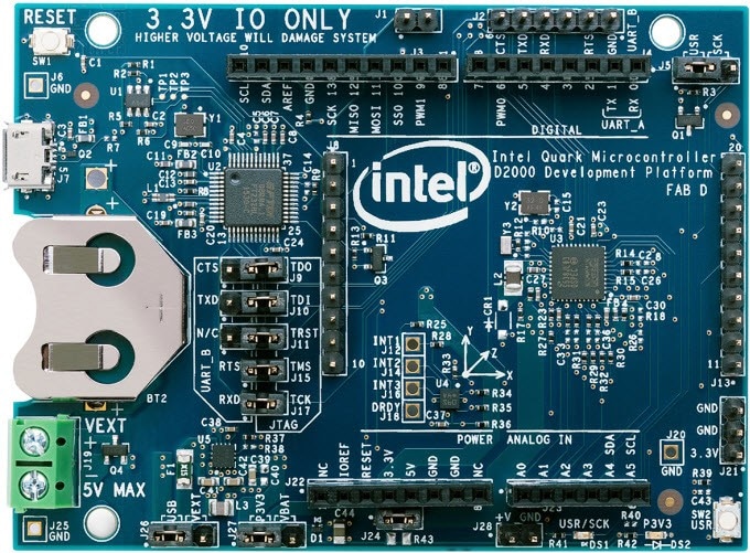
The floating point co-processor was removed from the Quark, presumably to lower the energy consumption. The 386 had around 275,000 transistors, and with the 486 having around 1.1million, some of that was due to the 8KB cache, although it's possible the Wikipedia figure uses the SX version rather than the DX with x87. But the Pentium had 3.3million (and 16KB of cache), so the size of the floating point is 2 million transistors at most, and likely under 500,000.
A GMA3150 is probably too large for a Pentium, but the i740 is listed as having 3,500,000 transistors:
| i740 | 3,500,000 | 1998 | Intel, Real3D | Real3D | 350 nm |
Model: i740
Date Released: 1998
Interface: AGP/PCI
Shader Model: N/A
DirectX: 6
Manufacturing Process: ?
Core Clockspeed: 55MHz
Memory Clockspeed: 100MHz
Memory Bus: 64-bit
Transistors: 3.5 million
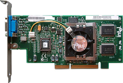
Intel i740 and GMA
"You're no doubt familiar with Intel's integrated GMA graphics that litter the low-cost landscape today, but did you know Intel also came out with a discrete 3D graphics chip? The year was 1998 and Intel had grand plans of competing in the 3D market, starting with the i740. Part of the reasoning behind the release was to help promote the AGP interface, and it was widely believed that Intel's financial status and manufacturing muscle would give the chip maker a substantial edge in competing with Nvidia and ATI.
Instead, poor sales and an underperforming product led Intel to abandon the discrete graphics market less than 18 months after it had entered, which also meant the i752 and i754 -- two followup GPUs -- would never see the light of day. And ten years after its launch, at least one site would look back at the i740 as one of "The Most Disappointing Graphics Chips in the Last Decade."
The original i740 design lives on, however, as it provided the basis for the much longer lasting GMA line, which still exists today. Moreover, Intel has on more than one occasion showed interest in re-entering the discrete graphics market, and its Larrabee architecture could see the light of day as early as this year.
Fun Fact: Sales of the i740 were so bad that some accused Intel of anticompetitive practices for allegedly seling its 740 graphics chips below cost to overseas videocard vendors in order to boost its market share."
Considering it had typically between 4-8MB of SDR RAM, that would be more than enough to run Windows 98 or a lightweight linux in the era of Mandrake or SuSE 7.0, even a later distro that didn't require a whole lot
Fun note: The i752 and i754 cores were later used for the integrated graphics in the Intel 810 and 815 chipsets, respectively. Intel no longer hosts i752 drivers, and advises users of i752-based cards to use the 810 drivers.[7]
Intel 810
The Intel 810 chipset was released by Intel in early 1999 with the code-name "Whitney"[1] as a platform for the P6-based Socket 370 CPU series, including the Pentium III and Celeron processors. Some motherboard designs include Slot 1 for older Intel CPUs or a combination of both Socket 370 and Slot 1. It targeted the low-cost segment of the market, offering a robust platform for uniprocessor budget systems with integrated graphics. The 810 was Intel's first chipset design to incorporate a hub architecture which was claimed to have better I/O throughput[2] and an integrated GPU, derived from the Intel740.[3]

There are five variants of the 810:
- 810-L: microATX (4 PCI), no display cache, ATA33 hard disk interface.
- 810: microATX (4 PCI), no display cache, ATA33 and ATA66.
- 810-DC100: ATX (6 PCI), 4 MB display cache (AIMM), ATA33 and ATA66.
- 810E: added support for 133MHz FSB, Pentium III or Celeron "Coppermine-EB" Series CPU.
- 810E2: added support for Pentium III and Celeron CPUs with 130 nm "Tualatin" core, ATA100 and 4 USB 1.1 ports.
Intel 810 attempted to integrate as much functionality into the motherboard as possible. Features include:[2][4]
- 66 and 100 MHz bus support
- 2 USB ports
- An integrated graphics processor.
- Based upon the Intel740 2D/3D accelerator (i752).
- Optional dedicated video RAM cache or use of system RAM.
- Hardware motion compensation for DVD playback.
- Digital video output
- AC'97 modem and audio
The hub design consisted of three chips, including the Graphics & Memory Controller Hub (GMCH), I/O Controller Hub (ICH), and the Firmware Hub (FWH). These components are connected by a separate 266 MB/s bus, double the previously typical 133 MB/s attachment via PCI-Bus. The added bandwidth was necessary because of increasing demands data transfer between components.[4]
The early GMCH (82810) chips (A2 stepping; S-spec numbers can be found on the fourth line of the chipset: SL35K, SL35X, SL3KK, SL3KL, Q790, Q789) could only support Celeron processors as they were unable to handle SSE instructions correctly.
810 supports asynchronous bus clock operation between the chipset and CPU (front side bus) and the system RAM. So, if the machine is equipped with a Celeron that uses only a 66 MHz bus, PC100 SDRAM can still be taken advantage of and will benefit the IGP.[4]
Boards based on the chipset do not have an AGP expansion slot, leaving the user to make do with PCI for video card options. 810-based boards include an AMR expansion slot. Additionally, the integrated graphics does not support 32-bit graphics mode, forcing the user to downsample the 810's standard 24-bit mode to 16-bit in order to run most games or full screen DirectX/OpenGL programs; many games will automatically downsample the output to 16-bit upon loading, however others will simply exit with or without an error or even crash due to the 24-bit mode not being supported by the game. The onboard graphics' performance in games was also unsatisfactory, and many games of that time had to be run at low resolution and low detail levels to be playable.
So it's likely that the i810 chipset used a lot more transistors than the 740 to accommodate many I/O buses like USB, but it's not impossible that many of the core features of later GMA and HD revisions can be found in the earliest integrated 840 series and still fit into 1mm^2. The cards are over 25 years old, so I am curious if the patents expired...I remember one of the first desktops that had a USB port- it was a Pentium II or III, and it had ONE USB 1.1 port in the back of the PC. It might have been a Pentium 3- and it was very useful for my portable MP3 player and digital camera, but it's amazing how times have changed- desktops now routinely include 4-10 USB ports including the back and front.


ARM Solutions (2012):
Microchip PIC24
The PIC24FJ256DA206 (Figure 1) 16-bit MCU features three graphics hardware accelerators to facilitate rendering of block copying, text and unpacking of compressed data and a color look-up table. The IC has 256 Kbytes of flash and 96 Kbytes of SRAM.
The chip also has an Enhanced Parallel Master Port (EPMP) for up to 16 Mbytes of external graphics RAM, if needed. This device has five timers, USB v2.0 On-The-Go, UART, SPI, and I2C I/O, 24 channels of 10-bit A/D conversion, and a real-time clock. It is said to be one of the lowest cost graphics solutions for QVGA and WQVGA displays.

Fujitsu MB86R01
The Fujitsu MB86R01 ‘Jade’ SoC (Figure 2) has a 32-bit ARM926EJ-S CPU core with a high-performance graphics display controller core with a 320 MHz internal memory frequency and enough performance for display resolutions up to 1024 x 768. It also features six layers of overlay window displays, with an alpha plane and constant alpha value for each layer, and two separate video-capture units that support YUV, RGB, ITU656, and other formats.
Jade targets automotive graphics applications, but is equally suited to many other high performance applications. The device features a hierarchical bus system that isolates high performance functions, such as 3D graphics processing, from routine operations such as low speed I/O. The ARM core runs at 333 MHz and the graphics core at 166 MHz. The external memory controller supports 302 MHz DDR2.
The chip supports two video inputs (YUV/ITU656 or RGB) and enables both upscaling and downscaling of a video image. It also can support two unique displays, and has two CAN ports, A/D and D/A converters, IDE, USB, SPI, FlexRay, and a Media LB port.

Atmel SAM9G
The Atmel SAM9G10 has an ARM926E-J-S core with DSP extensions and Java acceleration running at up to 400 MHz. It features an advanced graphics LCD controller with 4-layer overlay and 2D acceleration (picture-in-picture, alpha-blending, scaling, rotation, color conversion) and a 10-bit A/D converter that supports 4- or 5-wire resistive touchscreen panels. The chip has a 64-Kbyte ROM, 32 Kbytes of high-speed SRAM, and a 32-bit external bus memory interface supporting DDR2, static memories, and has circuitry for MLC/SLC NAND flash with ECC up to 24 bits. The device has no flash, but 32 Kbytes of fast ROM and 16 Kbytes of SRAM.
The SAM9G graphics controller supports 1 to 24 bits/pixel with scaling up to 800 x 600 pixels and has a 384-byte asynchronous output FIFO. The chip’s 10-layer bus matrix coupled with 2 x 8 DMA channels and dedicated DMAs for the communication and interface peripherals ensure uninterrupted data transfers with minimal processor overhead.
Multiple communication interfaces include a soft modem supporting the Conexant SmartDAA line driver, HS USB, FS USB Host, a 10/100 Ethernet MAC, two HS SDCard/SDIO/MMC interfaces, USARTs, SPIs, I2S and TWIs.
Texas Instruments AM3358
The Texas Instruments Sitara Am3358 Cortex-A8-based SoC is aimed at portable navigation devices, hand-held gaming and educational devices, home and building automation equipment, and other devices that require portability or low power consumption. It features a touch screen controller user interface, a 3D graphics accelerator (20 million triangles per second), an LCD display controller and 7 mW standby power. The LCD controller consists of two independent controllers, the raster controller and the LCD interface display driver (LIDD) controller
ARM graphics processing
Another thing you might consider is ARM Mali graphics. At present, this
graphics processor is used in a number of smart phones and tablet
computer SOCs, such as those for the Samsung Exynos 4212 phone and
Galaxy Tab, but it is not yet available in a microcontroller – stay
tuned. Obviously, one feature of Mali is very low power and, based on
the graphics quality of the end products mentioned, its performance is
good as well.
The integrated display controller is capable of directly driving almost
any LCD display with an RGB or STN/CSTN interface, which includes a wide
range of TFT, STN, and some OLED displays. These features effectively
create a complete graphical subsystem that is fully integrated on the
same chip as the MCU, driving up to 640 x 480 (VGA) display resolution.
So many options, so little time...
After reading the several ARM options, the way Intel standardizes their chipsets across platforms (at least within a generation) seems a lot less convoluted. Understandably, having an IP core to license from ARM isn't the same as needing to make a product compatible with customers at least wanting some semblance of standardized solutions.
That said, many of the Southbridge and Northbridge functions have been obsoleted by process shrinkage, which isn't to say it needs a lot more cruft. It's very likely that some rudimentary upgrades from the i810, perhaps including 32-bit graphics, which would support would benefit compatibility, and VRAM that isn't shared, such as eDRAM (call it eVRAM to distinguish it from system memory), without being too slow so that it is 4MB of discrete video and not using the precious system RAM.

A lot of the innovations of the Atom chipset were found in the Pentium M line, and transferred via the Stealey line. I was vaguely aware of the Pentium M in college- I had a roommate who had a desktop, or laptop with one, although I could never determine if it was faster than a Pentium IV or a dual core, but I realized it had some efficiency improvements. I checked if there were any laptops that used integrated GMA 915, and it seems like the Pentium M also used them:
The Pentium M processor, designed for laptops,did not support Hyper-Threading (HT); it prioritized power efficiency with features like SpeedStep, while HT was a hallmark of the desktop Pentium 4 (NetBurst architecture) for multitasking, though its benefits varied, with the later Core series vastly improving HT implementation. Hyper-Threading allows one physical core to act as two logical cores, improving throughput by using idle execution units, but early P4 versions sometimes saw slowdowns due to cache contention, a problem largely fixed in later Core processors.Key Differences & Features:
- Pentium M (Banias/Dothan): Focused on mobile efficiency, using the P6 architecture (like Pentium III) with a shorter pipeline, low power, and SpeedStep for dynamic clock scaling, but lacked HT.
- Pentium 4 (NetBurst): Aimed for high clock speeds with very long pipelines, and introduced Hyper-Threading (SMT) to make one core appear as two, boosting parallel performance.
- Hyper-Threading (HT): Duplicates instruction-tracking parts of a core, letting two threads run concurrently, filling execution units when one thread stalls.
- Performance Impact: While great for heavily threaded tasks (video editing, rendering), early P4 HT could hurt single-threaded apps due to shared resources like the cache, causing "cache thrashing".
In essence: If you have an older mobile CPU with "Pentium M" in the name, it doesn't have HT; if it's a "Pentium 4" or later "Core" processor, it likely does (or did, before Intel temporarily removed it from P-cores in newer designs)
While the Northbridge became obsolete, a redesign of the graphics bus to the CPU would not really cause a Northbridge-like bus to disappear in a modern process node.
https://book.huihoo.com/pc-architecture/chapter22.htm
But on reading about improvements to the NM10, a modern Northbridge isn't going to be discrete: The northbridge was replaced by the system agent introduced by the Intel Sandy Bridge microarchitecture in 2011, which essentially handles all previous Northbridge functions.[10] Intel's Sandy Bridge processors feature full integration of northbridge functions onto the CPU chip, along with processor cores, memory controller, high speed PCI Express interface and integrated graphics processing unit (GPU). This was a further evolution of the Westmere architecture, which also featured a CPU and GPU in the same package.[11] What if there is way to make all the IGP functions simplified for a very lightweight framebuffer. Containing many of the integrated functions, but for 256 colors instead of 24 bit, and far less cache. In other words, a Sandy bridge manufacturing process (32nm, GPU on same die) but using an Intel740-sized GPU (4MB). It would not, however, need any PCI-express, as most of the bandwidth would be under the GB/s speeds: https://en.wikipedia.org/wiki/Direct_Media_Interface In computing, Direct Media Interface (DMI) is Intel's proprietary link between the northbridge (or CPU) and southbridge (e.g. Platform Controller Hub family) chipset on a computer motherboard.[1] It was first used between the 9xx chipsets and the ICH6, released in 2004.[2]: 1 Previous Intel chipsets had used the Intel Hub Architecture to perform the same function, and server chipsets use a similar interface called Enterprise Southbridge Interface (ESI).[3] While the "DMI" name dates back to ICH6, Intel mandates specific combinations of compatible devices, so the presence of a DMI does not guarantee by itself that a particular northbridge–southbridge combination is allowed.
So I present to you, a Sandybridge-style IGP process, but for an i752 (a picture of the 810 was included since that was the first integrated Intel GPU chip that wasn't an AGP card) ported to 2-3nm:
"Today, we are moving into a period which could see a return to more custom architectures, driven primarily by low-power trends. Changes in processes technologies have also caused dynamic power to return to importance because the finFET resolves what had been a growing issue with leakage power. With a growing concern for dynamic power optimization, we may start to see more functions migrating away from general purpose processor solutions."
Edit 2-26-2026: Adding this paragraph from an 11-2025 article: https://semiengineering.com/the-next-big-thing/
If the Sandy Bridge is a technology that drove standardization forward, the acquisition of daily drivers has allowed developers to focus on more niche markets for systems that don't require their main PC. Thus it would appear that the embedded market could evolve to see fewer headless solutions and more graphics solutions, or the traditional chipmakers in the desktop market could seek to diversify away from bland AI marketing and revive their abandoned Medfield and Quark line of processors, adding eyes (GPU), ears (audio), and hands (keyboards and mice) back on to the faceless Mr. PotatoHead microcontrollers. Edit 3-11-2026: Another Quark economics article from 2013 I didn't see earlier: https://www.semiaccurate.com/2013/09/11/happens-shrink-p54c-pentium-32nm-call-quark/ "how many $5 not million devices would you have to make at what margins to pay for the masks alone? What odds do you see of hitting one out of the park like that? Would you risk it with your company?" "$5 chip is too powerful to run off a battery for multiple years. This means power is not a make or break proposition, nor is it a lever that people will pay notably more for." Except with Solar panels. "If you are paying $5000 for a wafer you need to get more than 1000 $5 devices off of it if you are going to make a positive return. That means about 50mm^2 or less per device, 250mm^2 on a $1000 -4 node wafer. Before you say that you can fit more transistors with higher performance on the $5000 wafer, if you are pin bound and don’t care about performance on that level, it is still a net loss." Except, if you port it to 2nm and yield 58,880 of them and sell them for $4 each. A 2nm wafer costs around $30,000. 1.6nm is $45000. The former would net around $202,000 (not including NREs). Manufacture 51,725 wafers for 3 billion people and your profits might be $9.575b (minus the $725m development cost). "For these reasons, Quark may be an OK fit for the intended market, may possibly be a viable business for Intel, but it makes no financial sense for anyone else to touch. It may fill fabs but what empty 32nm fabs does Intel have? Technically Quark may be an OK $5 32-bit controller with a non-industry standard ISA, financially though it makes no sense."
(Earlier, but similar concept- add Windows 98 or Linux 2.6, USB, and ONiO microcontroller keyboard+Exeger Solar )  https://www.youtube.com/shorts/axSQqnXpfko You can call it Quarkonomics. |


No comments:
Post a Comment